


 Call Us



Quick Answer
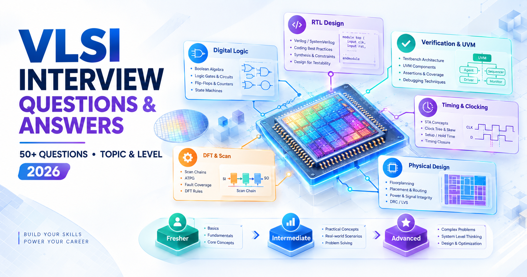
VLSI (Very Large Scale Integration) interviews test four layers of knowledge: digital logic and CMOS fundamentals, a hardware description language such as Verilog or SystemVerilog, a specialization (RTL design, verification with UVM, physical design, DFT, or low power), and practical debugging judgment through scenario questions. Freshers are mostly tested on combinational and sequential logic, number systems, and basic Verilog constructs, while experienced engineers face deep dives into static timing analysis, floorplanning, scan insertion, and low power intent files. This guide organizes more than 90 real interview questions by topic and experience level, with worked answers, so you can prepare in the order interviewers actually probe.
Key Highlights of VLSI Interview Questions
- VLSI interviews are layered: fundamentals for freshers, then a specialization track (design, verification, physical design, DFT, or low power) for anyone with 1+ years of experience.
- Setup and hold time, synchronous vs asynchronous logic, and combinational vs sequential circuits appear in almost every VLSI interview regardless of specialization.
- Verification roles increasingly test the Universal Verification Methodology (UVM), an Accellera-standardized, SystemVerilog-based framework, rather than plain testbenches.
- Physical design and DFT questions are scenario-driven: expect "what would you do if timing fails after routing" rather than pure definitions.
- The Semiconductor Industry Association projects a shortfall of tens of thousands of chip design and verification engineers through 2030, which is pushing companies toward more rigorous, multi-round technical screens.
- Low power design questions built around the IEEE 1801 Unified Power Format (UPF) standard are now common even at the fresher level, since almost every modern SoC is power-constrained.
What Is VLSI and Why Interviewers Test It This Way
VLSI stands for Very Large Scale Integration, the process of building integrated circuits by combining hundreds of millions to billions of transistors onto a single silicon die. It is the discipline behind every modern processor, memory chip, and system-on-chip (SoC). The field traces back to Gordon Moore's 1965 observation, now known as Moore's Law, that the number of components economically placed on a chip doubles at a regular interval; that single forecast, revised by Moore in 1975 to a two-year cadence, shaped decades of semiconductor roadmaps and is documented in detail by IEEE Spectrum's history of Moore's Law milestones.
Because a chip has to work correctly the very first time it comes back from the foundry (a single mask set can cost millions of dollars), VLSI teams are structured around distinct specializations, and interviews mirror that structure closely:
- RTL/Design engineers write the register-transfer-level code that describes chip behavior.
- Verification engineers prove that the RTL matches the specification before it ever reaches silicon.
- Physical design engineers turn verified RTL into a manufacturable layout (floorplan, placement, routing, timing closure).
- DFT engineers insert test structures so that manufacturing defects can be caught after fabrication.
- Analog/mixed-signal and low power engineers handle the parts of the chip that do not behave in clean digital 0s and 1s, and the power budget across the whole design.
An interviewer's first few questions almost always establish which of these tracks you are being evaluated for, then progressively narrows into your specific project experience. The sections below follow that same order, moving from universal fundamentals to specialization-specific and then experience-level questions.
Fresher Level: Digital Electronics and VLSI Fundamentals
These questions test whether your digital logic foundation is solid enough to build a specialization on top of. Expect them in the first 10 to 15 minutes of almost any VLSI interview, including experienced-level interviews, as a warm-up or a sanity check.
1. What is the difference between combinational and sequential circuits?
A combinational circuit's output depends only on the current values of its inputs; there is no memory element, so the same inputs always produce the same output regardless of history (examples: adders, multiplexers, decoders). A sequential circuit's output depends on both the current inputs and the circuit's stored state, which is held in memory elements such as flip-flops or latches (examples: counters, registers, finite state machines).
2. What is the difference between a latch and a flip-flop?
A latch is level-sensitive: it is transparent (output follows input) whenever its enable signal is active. A flip-flop is edge-triggered: it samples its input only at a clock edge (rising or falling) and holds that value until the next active edge. Flip-flops are preferred in synchronous digital design because they make timing analysis deterministic; latches are more area- and power-efficient but require careful timing borrowing analysis.
3. Explain setup time and hold time.
Setup time is the minimum interval before the active clock edge during which data must remain stable for it to be captured correctly. Hold time is the minimum interval after the active clock edge during which data must remain stable. A setup violation means data changed too close to (or after) the clock edge and can often be fixed by reducing clock frequency, using a faster cell, or reducing logic depth; a hold violation means data changed too soon after the capture edge and cannot be fixed by slowing the clock; it requires adding delay (buffers) on the data path instead.
4. What is metastability and how do designers handle it?
Metastability occurs when a flip-flop's setup or hold time is violated, typically because data crossing from one clock domain to another arrives at an unpredictable time relative to the receiving clock. The flip-flop's output can hover at an invalid voltage level for an unbounded time before resolving to 0 or 1. Designers mitigate this with multi-stage synchronizers (commonly two or three flip-flops in series) that give the metastable value time to resolve before it is used by downstream logic, along with proper clock-domain-crossing (CDC) verification.
5. What is the difference between Mealy and Moore state machines?
In a Moore machine, the output depends only on the current state. In a Mealy machine, the output depends on both the current state and the current input, which typically allows a Mealy machine to respond one clock cycle earlier and use fewer states, at the cost of being more prone to combinational glitches on the output.
6. Why is CMOS the dominant technology for digital VLSI?
CMOS (Complementary Metal-Oxide-Semiconductor) pairs an NMOS pull-down network with a PMOS pull-up network so that, in steady state, one network is always off. This gives CMOS near-zero static (leakage aside) power consumption, full-swing logic levels, and good noise margins compared to older NMOS-only or bipolar logic families, which is why it has been the backbone of digital chip design for decades.
7. What is fan-in and fan-out?
Fan-in is the number of inputs a logic gate has. Fan-out is the number of gate inputs a single gate's output is driving. High fan-out increases the load capacitance the driving gate must charge and discharge, which increases delay; designers manage this with buffer insertion or logic restructuring.
8. What is the difference between synchronous and asynchronous reset?
A synchronous reset only takes effect on an active clock edge, which keeps reset release timing predictable but requires the clock to be running for reset to work. An asynchronous reset takes effect immediately regardless of the clock, which resets the circuit even without a clock, but its release must be synchronized (using a reset synchronizer) to avoid creating a new metastability or recovery/removal timing problem.
9. What are the different types of memory used in VLSI, and how do SRAM and DRAM differ?
SRAM (Static RAM) stores each bit in a six-transistor cross-coupled latch and holds data as long as power is applied, with no refresh needed; it is fast but has a larger cell area, which is why it is used for on-chip caches. DRAM (Dynamic RAM) stores each bit as charge on a capacitor accessed through a single transistor, giving much higher density at lower cost per bit, but the charge leaks and must be periodically refreshed, which is why DRAM is used for main memory rather than caches.
10. What is the difference between Verilog and VHDL?
Both are hardware description languages used to model and simulate digital circuits. Verilog, standardized as IEEE 1364/1800, has a C-like, case-insensitive syntax and is generally considered faster to write for straightforward RTL. VHDL, an IEEE 1076 standard originally developed for the U.S. Department of Defense, is strongly typed and more verbose, which some teams value for catching errors at compile time. SystemVerilog, the modern superset of Verilog, added the object-oriented and assertion features used in verification, and the two original standards were merged in the 2009 revision.
RTL Design, Verilog, and SystemVerilog Questions
Once fundamentals are confirmed, most interviewers move into HDL-specific questions to test whether you can actually write synthesizable, bug-free RTL rather than just describe concepts.
11. What is the difference between blocking and non-blocking assignments in Verilog?
A blocking assignment (=) executes and updates its target immediately, in the order it is written, before the next statement runs; it is intended for combinational logic modeled inside an always block. A non-blocking assignment (<=) schedules the update to happen at the end of the current time step, so all right-hand sides are evaluated using pre-update values; it is the correct choice for modeling sequential (clocked) logic, because it accurately reflects how real flip-flops update simultaneously on a clock edge.
12. What is the difference between a task and a function in Verilog?
A function must execute in zero simulation time, cannot contain time-consuming statements such as #delay or wait, and must return exactly one value; it can be called from within an expression. A task can consume simulation time, can call other tasks and functions, and can have zero or more input, output, or inout arguments, but it cannot be used inside an expression.
13. What are the differences between wire and reg?
A wire represents a physical connection and must be continuously driven (for example by a module port or an assign statement); it cannot hold a value. A reg is a variable that holds its assigned value between procedural assignments inside an always or initial block. Despite the name, a reg does not always synthesize to a physical register; whether it becomes a flip-flop or combinational logic depends on the sensitivity list and coding style.
14. What is a race condition in RTL simulation, and how do non-blocking assignments help avoid it?
A race condition occurs when the simulation result depends on the order in which the simulator happens to evaluate statements that execute at the same simulation time, rather than on well-defined circuit behavior. Because non-blocking assignments defer the actual variable update until the end of the time step, using them consistently for sequential logic removes the order-dependence between multiple always blocks that read and write the same signals on the same clock edge.
15. What is the difference between casex, casez, and case?
case treats every bit literally, including X (unknown) and Z (high-impedance) values, so a bit must match exactly. casez treats Z values (and, by convention, ?) as don't-care during comparison. casex treats both X and Z as don't-care, which is convenient but risky in synthesis, because uninitialized (X) signals in simulation can silently match a case item that would not match in real hardware.
16. What is inferred versus instantiated logic?
Inferred logic is created automatically by the synthesis tool from behavioral RTL code (for example, writing an if-else that synthesis turns into a multiplexer). Instantiated logic is explicitly placed by the designer by naming a specific module or technology cell (for example directly instantiating a vendor's flip-flop or memory macro). Designers instantiate explicitly when they need a guaranteed structure, such as a specific memory macro, clock buffer, or scan-capable flip-flop.
17. What are generate blocks used for?
generate blocks let you create repeated or conditional hardware structures at elaboration time, for example instantiating N identical adder stages in a ripple-carry adder using a for-generate loop, or conditionally including a block of logic only for a certain parameter value. This keeps parameterized, reusable RTL far more compact than writing out every instance by hand.
18. What is the difference between parameter, localparam, and a `define macro?
parameter is module-scoped and can be overridden at instantiation time, making it ideal for reusable, configurable modules (for example a bus width). localparam is also module-scoped but cannot be overridden externally, so it is used for constants derived from other parameters. A `define macro is a global, compile-time text substitution handled by the preprocessor, with no type checking or scoping, which makes it easy to misuse across a large codebase.
Verification and UVM Interview Questions
Verification consumes the majority of the schedule on most modern chip projects, and companies increasingly standardize on UVM (Universal Verification Methodology), an Accellera-maintained, SystemVerilog-based class library that grew out of the Open Verification Methodology jointly developed by Cadence and Mentor Graphics, and was later contributed to the IEEE P1800.2 working group for ongoing standardization.
19. What is the difference between verification and validation in chip design?
Verification confirms that the design (RTL or gate-level netlist) correctly implements the specification, typically through simulation, formal methods, and emulation, before silicon exists. Validation confirms that the actual fabricated silicon works correctly in the real system and real use cases, using bring-up boards and system-level tests after tape-out.
20. Explain the basic components of a UVM testbench.
A typical UVM environment includes: a sequencer that generates sequences of stimulus items, a driver that converts those items into pin-level signals for the DUT (device under test), a monitor that passively observes DUT interface activity and converts it back into transactions, a scoreboard that compares observed behavior against an expected/reference model, and an agent that packages the sequencer, driver, and monitor together for one interface, all coordinated by an environment class and configured through a UVM test class.
21. What is the difference between directed testing and constrained-random verification?
Directed testing hand-writes specific stimulus sequences to exercise specific, known scenarios; it is precise but does not scale to the huge state space of a modern SoC. Constrained-random verification generates stimulus automatically within designer-specified constraints, letting the simulator explore corner cases a human might never think to write, and is typically paired with functional coverage to measure how much of the intended behavior has actually been exercised.
22. What is functional coverage, and how does it differ from code coverage?
Code coverage (line, statement, branch, toggle, FSM state coverage) measures how much of the RTL code's structure has been exercised by simulation; it says nothing about whether the important functional scenarios were tested. Functional coverage is explicitly written by the verification engineer using covergroup constructs to track whether specific, meaningful combinations of values and scenarios (defined from the specification) actually occurred, which is a much stronger signal of verification completeness.
23. What is a scoreboard, and how does it detect a bug?
A scoreboard is a verification component that predicts expected DUT behavior, usually via a reference model or golden algorithm, and continuously compares that prediction against the transactions actually observed at the DUT's outputs by the monitor. Any mismatch is flagged as a functional bug. Scoreboards are what let constrained-random tests self-check without a human reviewing waveforms for every run.
24. What is the difference between simulation, emulation, and formal verification?
Simulation runs the RTL in software against a testbench, cycle by cycle; it is flexible but slow, especially for large SoCs. Emulation maps the design onto specialized hardware (an FPGA-based or custom emulator) to run orders of magnitude faster, which is essential for software bring-up and long test sequences. Formal verification uses mathematical proof techniques to exhaustively check whether a design satisfies a property (an assertion) for all possible input sequences, without needing any testbench stimulus at all, which makes it especially effective for control logic and corner cases that are hard to hit with random simulation.
25. What is an assertion, and what is the difference between an immediate and a concurrent assertion?
An assertion is a statement that checks whether a design property holds, flagging a violation automatically instead of relying on a scoreboard or manual waveform review. An immediate assertion is checked like a procedural statement, evaluated once when execution reaches it (similar to an if check). A concurrent assertion, written using SystemVerilog Assertions (SVA), is evaluated over time relative to a clock, checking temporal sequences (for example "if a request is asserted, a grant must follow within four cycles").
26. What is clock domain crossing (CDC), and why does it need special verification?
CDC occurs whenever a signal moves from logic clocked by one clock to logic clocked by a different, asynchronous clock. Because the two clocks have no fixed phase relationship, standard static timing analysis cannot verify these paths, and a signal can be sampled mid-transition, causing metastability. CDC verification uses dedicated static tools that check for proper synchronizer structures (such as two-flip-flop synchronizers, or handshake/FIFO-based crossings for multi-bit buses) on every clock-crossing path in the design.
Static Timing Analysis and Clocking Questions
Static timing analysis (STA) questions appear heavily in physical design, STA-specialist, and mixed-signal interviews, since timing closure ultimately decides whether a chip meets its target frequency.
27. What is static timing analysis, and how is it different from timing simulation?
STA analyzes every timing path in a design (input to register, register to register, register to output) against the clock constraints, checking setup and hold requirements without applying any test vectors; it exhaustively covers every path in the design in one run. Timing simulation only checks the specific input patterns you apply, so it can miss paths that were never exercised, but STA has no notion of functional correctness, only whether a signal arrives in time.
28. What is slack, and what does negative slack mean?
Slack is the difference between the required arrival time for a signal and its actual (estimated) arrival time. Positive slack means the path meets timing with margin to spare; negative slack means the path is too slow (a setup violation) or, for hold checks, that data is arriving and changing too soon (a hold violation), and the chip will not function correctly at the target clock frequency until it is fixed.
29. What are the main techniques to fix a setup violation?
Common fixes include: reducing logic depth on the path (restructuring or re-pipelining), using higher-drive-strength or lower-threshold-voltage cells to speed up the path, resizing gates, reducing wire load through better placement, or as a last resort, reducing the overall clock frequency. Adding an extra pipeline stage (register) is often the most robust long-term fix if the path is fundamentally too long.
30. What are the main techniques to fix a hold violation?
Since hold violations do not depend on clock frequency, they are fixed by adding delay to the data path, typically by inserting buffer/delay cells, since slowing the clock cannot fix them the way it can fix setup. Hold fixes are usually applied late in the physical design flow, after routing, when actual wire delays are known.
31. What is clock skew, and what is the difference between positive and useful skew?
Clock skew is the difference in arrival time of the same clock edge at two different flip-flops, caused by differences in clock network wire length and buffering. Positive skew (clock arrives later at the capture flop than the launch flop) helps setup timing but hurts hold timing; negative or "useful" skew intentionally shifts clock arrival to help a specific critical path meet setup at the cost of hold margin elsewhere, and is a deliberate optimization technique used late in the physical design flow.
32. What is jitter, and how does it affect timing margin?
Jitter is the cycle-to-cycle variation in the actual period of a clock signal, caused by noise in the clock generation and distribution (such as a PLL). Because jitter makes the exact clock edge position uncertain, timing tools subtract a jitter margin from the available timing budget, effectively reducing the usable clock period even though the nominal frequency stays the same.
33. What is a false path and a multicycle path, and why do they matter?
A false path is a timing path that physically exists in the netlist but can never actually be sensitized during real operation (for example, between two mutually exclusive configuration modes), so it should be excluded from timing analysis to avoid wasting optimization effort or reporting a fake violation. A multicycle path is a path that is only required to settle over more than one clock cycle (common in slower control logic), which must be explicitly constrained, or STA will incorrectly flag it as a single-cycle setup violation.
Physical Design, Floorplanning, and Place and Route
Physical design turns a verified, synthesized netlist into a manufacturable layout. Interviewers here weigh practical judgment (what would you check first) as heavily as terminology.
34. What are the major stages of the ASIC physical design flow?
A typical flow proceeds through: floorplanning (deciding chip area, macro placement, power planning), placement of standard cells, clock tree synthesis (CTS), routing (global and detailed), and timing/physical signoff, followed by tape-out to the foundry. Each stage feeds timing and congestion estimates back to earlier stages, which is why physical design is iterative rather than strictly linear.
35. What is floorplanning, and why does it matter so much for final quality of results?
Floorplanning defines the chip's overall area, the placement of large macros (memories, IP blocks), and the initial power and ground network. Because floorplanning decisions constrain everything downstream, such as wire lengths, congestion, and power delivery, a poor floorplan can make timing closure or routing essentially impossible later, no matter how much effort is spent on placement or routing optimization.
36. What is congestion, and how is it typically resolved?
Congestion occurs when the number of wires that need to route through a region of the chip exceeds the available routing resources in that region, leading to detours, longer wires, and worse timing. It is typically resolved by adjusting placement density, adding routing blockages strategically, resizing or moving macros during floorplanning, or, if severe, by increasing the chip's die area.
37. What is clock tree synthesis (CTS), and what is it trying to optimize?
CTS builds the buffered distribution network that delivers the clock signal from its source to every sequential element in the design. Its goals are to minimize clock skew (so all flops see the clock edge at nearly the same time), minimize insertion delay and clock power, and keep the network robust to on-chip variation, all while meeting the overall floorplan's routing and area constraints.
38. What is an antenna effect, and how is it fixed?
During fabrication, long metal wires connected to a transistor gate can act like an antenna, accumulating charge from plasma-based etching processes before the rest of the circuit (including protective diodes) is fully connected; this charge can damage the thin gate oxide. It is fixed by adding antenna diodes to safely discharge accumulated charge, or by "jumping" the wire to a higher metal layer partway through routing to break up the charge accumulation path.
39. What is IR drop, and why does it matter?
IR drop is the voltage drop across the power delivery network's resistance as current flows through it, meaning transistors far from a power source effectively see a lower supply voltage than intended. Excessive IR drop slows down transistor switching (hurting timing) and, in extreme cases, can cause functional failures; it is managed through wider power straps, more power/ground vias, and decoupling capacitors placed near high-switching-activity blocks.
Design for Testability (DFT), Scan, and ATPG Questions
DFT ensures that manufacturing defects, which have nothing to do with logical correctness, can still be caught after a chip comes back from the fab. These questions are common for DFT specialists but also show up as a section in general physical design and verification interviews.
40. Why does a functionally correct design still need DFT?
Verification proves the design is logically correct; it says nothing about whether an individual manufactured chip has a physical defect (a short, an open, a stuck transistor). DFT structures exist purely to test each fabricated die for these manufacturing defects quickly and with high confidence, which is a completely separate problem from functional correctness.
41. What is a scan chain, and how does scan insertion work?
Scan insertion replaces normal flip-flops with scan flip-flops, which have an added multiplexer that can select either normal functional data or a serial scan-in bit. These scan flip-flops are then chained together, output to input, forming a shift register that lets an external tester shift arbitrary test patterns directly into internal state, and shift the resulting captured state back out, giving controllability and observability that would otherwise be impossible for deeply buried internal logic.
42. What is ATPG, and what is stuck-at fault coverage?
ATPG (Automatic Test Pattern Generation) is software that automatically generates the minimal set of test patterns needed to detect modeled manufacturing faults, most commonly the stuck-at fault model, where a signal is assumed to be permanently stuck at logic 0 or logic 1. Stuck-at fault coverage is the percentage of all possible stuck-at faults in the design that the generated pattern set can actually detect; most tape-out signoff criteria require coverage at or above roughly 95 to 99 percent.
43. What is BIST, and what is the difference between MBIST and LBIST?
BIST (Built-In Self-Test) embeds test generation and response-checking logic directly on the chip, so it can test itself without an external tester driving every pattern. MBIST (Memory BIST) targets embedded memories, applying algorithms such as March tests to catch memory-specific defects. LBIST (Logic BIST) targets general logic, typically using an on-chip pseudo-random pattern generator and a signature-compacting response analyzer, and is especially valuable for in-field, periodic self-testing in safety-critical applications such as automotive chips.
44. What is JTAG, and what is it used for in a chip beyond just testing?
JTAG, standardized as IEEE 1149.1, defines a standard serial Test Access Port (TAP) and boundary-scan architecture originally built for testing interconnects on a printed circuit board. On modern chips it is also widely reused as the access mechanism for silicon debug, programming on-chip fuses, and even loading configuration data, in addition to its original boundary-scan test role.
Low Power Design: UPF, Clock Gating, and Power Gating
Almost every modern SoC, from a battery-powered wearable to a data-center AI accelerator, is power-constrained, which is why low power questions now appear even in fresher interviews.
45. What are the two main components of chip power consumption?
Total power is the sum of dynamic power and leakage (static) power. Dynamic power is consumed when transistors switch state and is roughly proportional to switching activity, load capacitance, supply voltage squared, and clock frequency. Leakage power is consumed even when transistors are not switching, due to current that leaks through transistors that are nominally off, and it has grown steadily more significant as transistor dimensions have shrunk.
46. What is clock gating, and how does it save power?
Clock gating inserts a gating cell (commonly an integrated clock gating cell, or ICG) that disables the clock to a register or block of registers when that logic is not going to change state on the next cycle, preventing wasted switching (and therefore wasted dynamic power) in flip-flops that do not need to toggle. It is one of the most widely used and highest-return low power techniques because it requires no change to functional behavior.
47. What is power gating, and what design elements does it require?
Power gating shuts off the supply voltage entirely to a block that is idle, using header or footer switch cells, which eliminates leakage power in that block almost completely while it is off. Because internal signal states are lost when power is removed, power-gated blocks typically need retention registers to preserve critical state, isolation cells to hold outputs at a known value while the block is off (so downstream logic does not see floating or glitching signals), and a controlled power-up sequence to avoid inrush current problems.
48. What is UPF, and what does it actually specify?
UPF (Unified Power Format), standardized as IEEE 1801, is a Tcl-based specification language used to describe "power intent" separately from functional RTL: it defines power domains, which supply nets feed which domains, retention and isolation strategy, and the legal power state combinations across the chip. Keeping this in a separate file lets the same RTL be reused across designs or process nodes with different power architectures, and lets verification, synthesis, and physical design tools all consume one consistent power specification.
49. What is a level shifter, and when is it needed?
A level shifter converts a signal from one voltage domain to another whenever a signal crosses between two power domains operating at different voltages, since a logic-high signal at a lower voltage may not be reliably recognized as high by circuitry running at a higher voltage, and vice versa. Missing a required level shifter is a common and serious low power design bug that low power verification tools specifically check for.
ASIC vs FPGA: Questions Interviewers Love to Ask
Many candidates have used FPGAs in coursework but are interviewing for ASIC roles, so interviewers often probe this comparison directly to check real understanding of the tradeoffs.
50. What is the fundamental difference between an ASIC and an FPGA?
An ASIC (Application-Specific Integrated Circuit) is custom-fabricated silicon where the transistors and interconnects are laid out specifically to implement one design; it cannot be changed after fabrication. An FPGA (Field-Programmable Gate Array) is a pre-fabricated chip full of generic, reconfigurable logic blocks and routing that can be reprogrammed after manufacturing to implement many different designs.
| Aspect | ASIC | FPGA |
|---|---|---|
| Non-recurring engineering cost | Very high (mask sets, verification effort) | Low to none |
| Per-unit cost at high volume | Low | Higher (pre-built silicon overhead) |
| Performance and power | Optimized for the specific design | Lower, due to generic reconfigurable fabric |
| Time to market | Long (months for tape-out and fab turnaround) | Short (reprogram in minutes) |
| Post-fabrication changes | Not possible | Fully reprogrammable |
51. Why do some teams prototype on FPGA before committing an ASIC design to tape-out?
FPGA prototyping lets teams validate that RTL behaves correctly at real (or near-real) speed, including running actual embedded software on it, long before the far more expensive and time-consuming ASIC fabrication step. Bugs caught on an FPGA prototype are dramatically cheaper to fix than the same bugs discovered after silicon is already fabricated.
52. Why can't FPGA logic simply be "converted" into an ASIC with no extra work?
FPGA designs rely on the specific reconfigurable fabric (look-up tables, dedicated hard blocks) of the target FPGA family, and an FPGA-oriented RTL coding style is often not optimal for standard-cell ASIC synthesis. Moving to ASIC typically requires re-verifying timing against a completely different technology library, redesigning any FPGA-specific hard IP usage (such as vendor-specific memory or DSP blocks) with equivalent custom or licensed IP, and running a full physical design flow that has no FPGA equivalent.
Experienced and Lead-Level Scenario Questions
Beyond definitions, experienced and lead-level interviews focus on judgment: how you diagnose and prioritize problems under real project constraints such as schedule pressure and incomplete information.
53. A block passes all functional simulation but fails on the actual silicon. How would you debug this?
A strong answer walks through a structured elimination process: first confirm whether the failure is systematic (every chip) or a subset (pointing to a process-corner or manufacturing defect issue), check whether the failure correlates with voltage, temperature, or frequency (suggesting a timing margin or signal integrity issue not modeled in simulation), review whether DFT/scan patterns still pass (isolating whether it is a structural defect versus a design issue), and check for known simulation-to-silicon gaps such as unmodeled parasitic effects, clock domain crossing bugs that only manifest probabilistically, or an incorrect power intent assumption.
54. Timing closure looks impossible on a block: many paths are failing setup after place and route. What is your prioritized approach?
Rather than attacking every failing path individually, an experienced engineer first checks whether the floorplan itself is the root cause (bad macro placement causing systematically long routes), looks for a small number of structurally difficult paths (such as a path crossing many hierarchical boundaries or a poorly pipelined multiplier) that are dragging overall numbers down, and considers whether re-pipelining, re-floorplanning, or renegotiating the target frequency with the architecture team is more effective than incremental cell-level fixes across hundreds of individually marginal paths.
55. How do you decide the right verification strategy (directed vs constrained-random vs formal) for a given block?
Control-heavy logic with a small, well-defined state space (arbiters, FSMs, protocol handshakes) is often a strong candidate for formal verification, since it can be exhaustively proven. Data-path-heavy or highly parameterized blocks (a large crossbar, a wide bus fabric) are usually better suited to constrained-random simulation with functional coverage, since formal tools can struggle with state-space explosion there. Directed tests remain valuable for specific known corner cases, especially compliance to an external spec, and for basic sanity/regression coverage early in the project before random testing infrastructure is mature.
HR and Behavioral Questions for VLSI Roles
Technical rounds are usually followed by an HR or managerial round, where companies assess communication, teamwork, and fit rather than raw technical depth.
- "Walk me through a bug you found that others had missed, and how you found it." Interviewers want a structured narrative: what symptom you noticed, what you ruled out, and how you isolated the root cause, not just the final fix.
- "How do you handle disagreement with a senior engineer about a design decision?" A good answer shows you can back a position with data (simulation results, timing reports, coverage numbers) rather than opinion, while remaining open to being wrong.
- "Describe a time you had to meet a tight tape-out deadline." Interviewers are probing prioritization under pressure and whether you know when to escalate a risk rather than silently absorbing it.
- "Why are you interested in this specialization (design, verification, physical design, or DFT) specifically?" A shallow "I'm interested in chips" answer is a red flag; a strong answer references a specific project or coursework experience.
For general behavioral question patterns and how to structure your answers using frameworks such as STAR, Simpliaxis's broader HR interview questions and answers guide is a useful companion resource alongside the technical preparation above.
VLSI Salary and Job Market Outlook in 2026
The semiconductor industry is in a genuine hiring crunch for design and verification talent. The Semiconductor Industry Association's 2023 "Chipping Away" workforce study, conducted with Oxford Economics, projected that the U.S. semiconductor industry, which employed roughly 345,000 workers at the time of the study, would need to add around 115,000 more jobs by 2030, and that at current graduation and training rates, tens of thousands of those roles, the large majority of them engineers and computer scientists rather than technicians, risked going unfilled. That structural shortage, combined with continued CHIPS Act-driven fab investment and surging AI chip demand, is a major reason semiconductor employers now run multi-round technical interviews rather than a single generalist screen.
On compensation, salary aggregator data (such as Glassdoor's crowd-sourced VLSI design engineer figures) should be read as directional rather than exact, since self-reported salary data varies by seniority mix, region, and company tier within any given sample. Broadly, VLSI-specific roles such as physical design, DFT, and verification engineering command a premium over generalist electronics engineering roles, and that premium widens with seniority as engineers move from RTL/testbench-level work into architecture and signoff ownership. In the United States, the U.S. Bureau of Labor Statistics' Occupational Outlook Handbook tracks the broader "Electrical and Electronics Engineers" occupational category (which includes many but not all VLSI-specific job titles) and projects continued, faster-than-average employment growth for the category through the mid-2030s, driven substantially by demand in semiconductors, defense electronics, and computing hardware.
Specialization also affects compensation trajectory over a career. Entry-level RTL design and verification roles tend to have the largest fresher hiring pools and the most standardized interview loops, while physical design, DFT, and low power specialists, who become scarcer as designs move to advanced process nodes, often see the steepest salary growth after the first two to three years of experience, largely because there are fewer engineers who have hands-on signoff experience at cutting-edge nodes.
Key Takeaways
- VLSI interviews are structured in layers: universal digital logic and CMOS fundamentals first, then a specialization track, then experience-level scenario and debugging questions.
- Setup/hold time, blocking vs non-blocking assignments, and combinational vs sequential logic are asked across almost every specialization and experience level, so master them first.
- Verification interviews increasingly test UVM (an Accellera/IEEE-standardized methodology) rather than ad hoc testbenches; know the sequencer, driver, monitor, and scoreboard roles cold.
- Physical design and DFT questions are scenario-driven in practice; practice explaining your debugging process, not just definitions.
- Low power design knowledge (UPF, clock gating, power gating, level shifters) is now expected even at fresher level, since nearly every modern chip is power-constrained.
- The semiconductor industry faces a well-documented, multi-year talent shortage in design and verification roles, which is both a strong career tailwind and the reason interview loops have gotten more rigorous.
- Preparation should be timeline-adjusted: with limited time, prioritize fundamentals plus your single target specialization over shallow coverage of everything.
How to Prepare: A Study Plan by Timeline
If you have one month
- Week 1: Rebuild digital logic and CMOS fundamentals from scratch; do not skip this even if you "already know it," since interviewers use it to gauge depth of thinking, not just recall.
- Week 2: Pick your target specialization (design, verification, physical design, or DFT) and go deep on that section of this guide rather than trying to master all five.
- Week 3: Practice writing small RTL modules and, if targeting verification, a small UVM testbench from scratch, since many interviews now include a live coding round.
- Week 4: Do mock interviews focused on scenario and debugging questions (see the experienced-level section above), since these differentiate strong candidates far more than definitions do.
If you have one week
- Focus entirely on the fundamentals section and your target specialization's section; skip the others.
- Rehearse two or three real project stories out loud, since almost every interview asks you to walk through your own past work in detail.
- Review your resume's project section line by line and be ready to defend every technical claim on it; vague resume bullet points are one of the most common sources of a bad interview.








 Lowest-Price Challenge











 Personalized Path


.webp)


 USA
USA  Canada
  India
India  UK
UK  Australia
  Singapore


